At a glance
- Qualcomm today is announcing that they have completed initial validation on their High Bandwidth Compute technology
- The DRAM-stacked-upon-compute architecture moves on to commercialization, with Dragonfly AI250 set to sample in the first half of 2027
# Qualcomm Validates HBC Stacked Memory Ahead of 2027 Dragonfly AI250 Sampling
Qualcomm has completed initial validation of its High Bandwidth Compute (HBC) memory architecture, a key component of the company’s upcoming Dragonfly data center AI accelerators. The technology is slated for commercial sampling next year as part of the Dragonfly AI250 accelerator and its successors.
HBC Architecture: Compute at the Base of the Stack
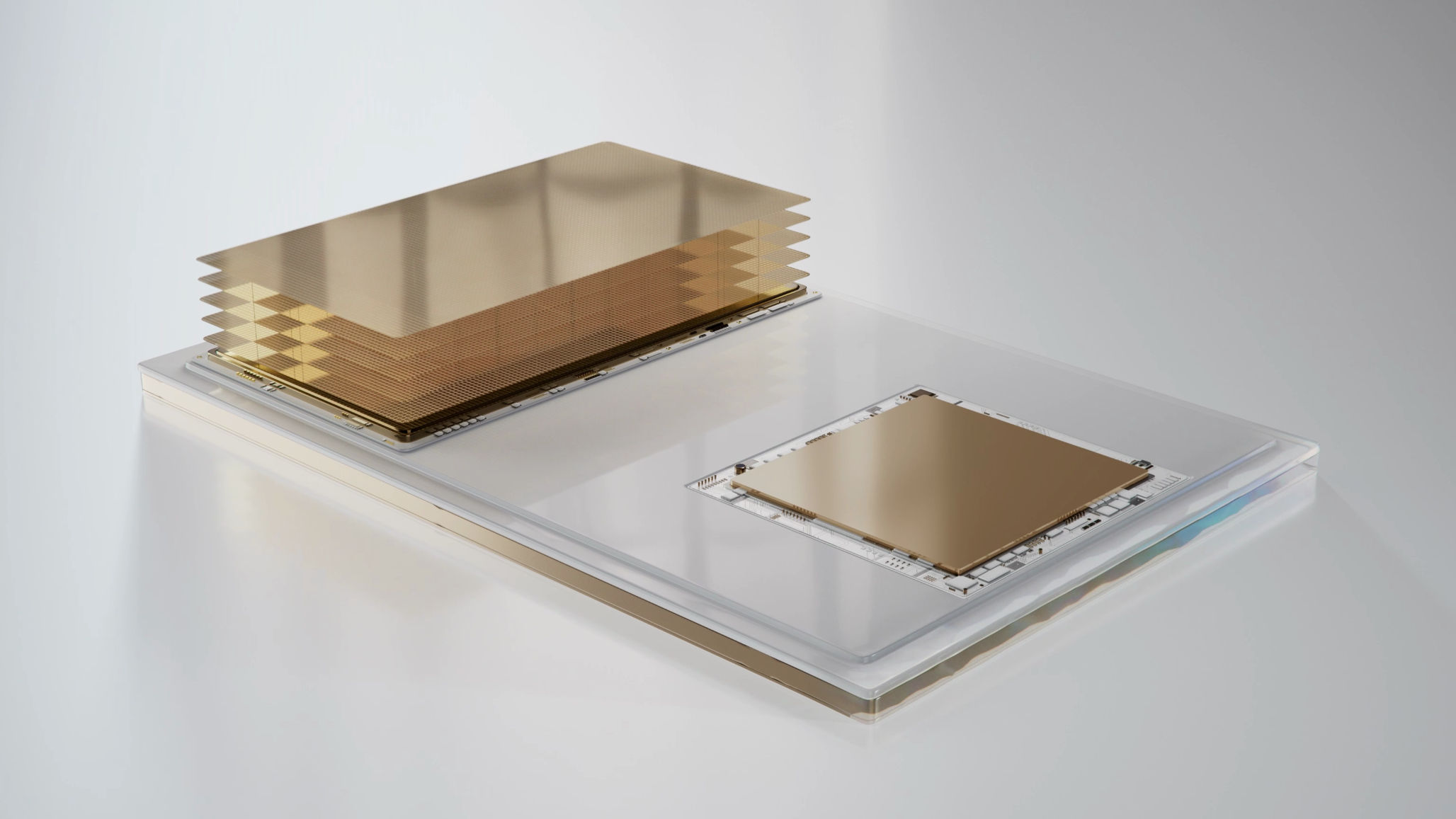
HBC represents Qualcomm’s approach to near-memory compute, designed to balance memory capacity, memory performance, and production costs. The architecture builds on memory stacking principles similar to High Bandwidth Memory (HBM), but with a fundamental structural difference. In conventional HBM, multiple DRAM dies are stacked atop a base die that connects to a host processor through an ultra-wide memory bus. HBC instead places a small compute die at the bottom of the stack, with DRAM layers positioned directly on top.
This arrangement minimizes the distance data must travel between memory and compute. By eliminating even the relatively short connection used in HBM—and avoiding external memory such as LPDDR5X entirely—Qualcomm aims to reduce the energy spent moving data. Those savings can be reinvested into chip performance or used to cluster more chips within the same energy footprint.
The compute die under the memory is not a full processor. Rather, it handles the most memory bandwidth-intensive operations, sending results back to a larger central compute die within the processor package.
Cost and Manufacturing Trade-offs
Qualcomm is also targeting production cost reductions with HBC. Standard HBM requires advanced packaging such as CoWoS or EMIB to connect memory stacks to compute dies and memory controllers because of the wide memory bus involved. By shifting most computational workloads to the compute die beneath the memory stack, far less bandwidth is needed to link that die to a larger processor die elsewhere in the package. Qualcomm states this connection can be built using cheaper traditional 2D organic substrates.
The architecture is not free of manufacturing complexity. Like HBM, HBC requires bonding multiple DRAM dies—or wafers in Qualcomm’s implementation—on top of another die using through-silicon vias (TSVs). Qualcomm notes that while complex manufacturing techniques remain necessary, the challenge is reduced from both memory stacking and high-speed chiplet connectivity to just the memory stacking.
On capacity, Qualcomm’s HBC design uses LPDDR5X DRAM dies rather than the thin, high-performance dies used in HBM. The company has not disclosed final performance figures, but it projects that an HBC stack will offer larger capacity than current HBM4 implementations.
Validation Results: 5x Bandwidth-per-Watt Over HBM4
For initial validation, Qualcomm connected an early HBC sample stack to a test unit in its San Diego labs. The test stack contained two layers of DRAM dies; shipping products are planned with four layers, so Qualcomm is not yet testing full-sized stacks.
Using an automated tester, Qualcomm measured the stack both as an LPDDR5X device and as an HBC device. The company reported three major findings:
- The technology works, proving the approach is viable.
- HBC delivered more than five times the energy efficiency of HBM4 on a bandwidth-per-watt basis, according to HBM4’s own specifications.
- Measured bandwidth was 18 times higher than external LPDDR5X.
Qualcomm did not disclose specific bandwidth figures. The energy efficiency result falls short of the company’s initial projection of beating HBM by 6x, but Qualcomm indicates it still represents a significant improvement if carried into a full product. Validation testing also included thermal behavior, though the company provided no further detail.
Operator Implications and Market Context
For data center operators evaluating AI inference infrastructure, HBC addresses a central constraint: memory bandwidth and capacity often limit inference performance. Qualcomm positions HBC as offering better bandwidth than external LPDDR and approaching HBM, without the capacity constraints of on-die SRAM or the high cost of advanced packaging.
If the efficiency and capacity projections hold in volume production, HBC could allow operators to deploy more AI inference compute within fixed power envelopes. The use of LPDDR5X dies and 2D organic substrates may also ease supply chain and cost pressures compared with HBM-dependent designs that rely on CoWoS or EMIB capacity.
Sampling of the Dragonfly AI250 is expected next year, with mass production targeted thereafter. Until shipping products arrive, operators will have to weigh Qualcomm’s projected gains against validated results from a two-layer test stack rather than a four-layer commercial product.

MegaWatt Intelligence Desk
Hyperscale & Grid Analyst. `More stories by $MegaWatt Intelligence Desk →`