At a glance
- Demand for advanced chips is rising
- The processes to build them are getting more complex
- And the margin for error is shrinking
- For engineers, understanding how a process change will behave, how a material will interact with a new step, how a defect maps back to a root cause are critical, challenging steps in semiconductor…
# The AI-Defined Fab: How Accelerated Computing Is Reshaping Semiconductor Manufacturing
Semiconductor manufacturing is entering a new phase. As advanced chip demand rises and process complexity increases, the margin for error is shrinking. For process engineers, understanding how a material will interact with a new step or how a defect maps back to a root cause remains critical—but these analyses have traditionally taken days. Physical experiments on a fab line are slow and expensive, and a wrong call on yield or process quality carries real consequences.
Artificial intelligence is now transforming how engineers approach these challenges. By shortening simulation times, predicting process behavior without full computational runs, and automating sequences of engineering tasks, AI is helping teams evaluate more alternatives before committing to physical trials. The result is what industry participants are describing as an AI-defined fab: a manufacturing environment where AI supports process optimization, earlier problem detection, and better decision-making across the full chip lifecycle.
Shorter Simulation Cycles Expand Engineering Options
Accelerated computing does more than speed up individual calculations—it changes how many alternatives engineers can test before moving to physical hardware. Multiphysics simulations, which model interactions among heat transfer, electrical behavior, and mechanical stress, are central to semiconductor equipment and process optimization.
Simulation software provider COMSOL is using the NVIDIA cuDSS library to accelerate multiphysics simulations for semiconductor manufacturing by up to 10x. That acceleration allows engineers to compare more alternatives and decide which changes warrant physical testing.
Applied Materials and NVIDIA are collaborating on atomic-scale materials discovery and process development. By integrating NVIDIA cuDSS into Applied’s Ginestra simulation platform, the company achieves performance up to 10x faster than CPU-only approaches. With NVIDIA PhysicsNeMo, Applied’s ACE+ multiphysics platform delivers topography simulations up to 35x faster.
In some cases, acceleration enables calculations that were previously impractical. Computational lithography, which defines how circuit patterns are printed onto silicon, involves calculations too intensive to complete on CPU at production scale. Siemens is integrating NVIDIA cuLitho into its Calibre lithography software, delivering up to 17x acceleration on key simulation workloads. That expansion of verifiable scenarios gives engineers more confidence before a wafer goes to print.
Physics-Based AI Predicts Behavior Without Full Simulations
Beyond accelerating simulations, AI trained on physics can predict how materials and processes will behave without running a full simulation each time. The payoff is most visible in complex calculations that remain expensive even on accelerated hardware.
Plasma—the electrically charged gas used in semiconductor etch processes—is one example. Modeling plasma behavior requires solving equations that capture how electrical, chemical, and thermal processes interact, making repeated simulation costly. NVIDIA PhysicsNeMo can assist in reducing plasma-prediction simulation time from days to as little as milliseconds.
Lam Research intends to integrate NanoVDB into its advanced semiconductor process modeling platform SEMulator3D, part of the company’s Semiverse Solutions family of virtual products. The addition of NanoVDB is expected to accelerate select wafer-etch modeling by up to 30x.
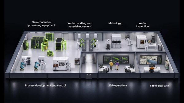
Applied Materials is using digital twins built on NVIDIA Omniverse libraries to simulate fab-level optimizations in layout, throughput, cost, and process control.
AI Agents Handle the Steps Between Decisions
Engineers turn analyses into decisions—revising a design, investigating a test failure, or adjusting a production process. AI agents can help carry out the steps between those decisions.
Evaluating which AI model to apply to a given task is one example: a sequential, manual process that can consume hours on the test floor. Advantest is using NVIDIA NeMo Switchyard AI agents to automate that selection, reducing response times from hours to minutes.
Digital Twins Test Factory Changes Before They Reach the Line
Digital twins let teams simulate equipment configurations, layouts, and process changes in a virtual environment before committing to physical trials. This reduces experimentation costs, especially as fabs become more complex and the stakes of a wrong change get higher.
Applied Materials uses NVIDIA Omniverse libraries to build physically accurate digital twins of entire fabs. Teams can simulate material movement, identify bottlenecks, and evaluate layouts and operating strategies—extending virtual experimentation beyond individual processes to how the factory works as a whole.
The Connected Loop
The future of semiconductor manufacturing lies in connecting these capabilities: using production data to inform models and models to evaluate changes, then bringing those findings back to the engineers making production decisions.
That is the promise of the AI-defined fab—where AI helps people learn from each production cycle and act on that knowledge sooner. Engineers direct the work and make decisions based on their expertise while spending less time waiting for answers.

MegaWatt Intelligence Desk
Hyperscale & Grid Analyst. `More stories by $MegaWatt Intelligence Desk →`